-
Phone
86-755-2****
-
Address
Block B, No. 8 Mingfu Road, Shatou Industrial Zone, Shajing Town, Baoan District, Shenzhen, Guangdong, China
-
E-mail
LatestProducts


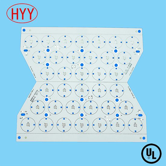
Profile by Routing LED PCB with Outdoor Lamp
Circuit Board, PCB Board, PCB
Description
Basic Info
- Model NO.: hyy-007
- Flame Retardant Properties: V0
- Base Material: Aluminum
- Processing Technology: Electrolytic Foil
- Mechanical Rigid: Rigid
- Brand: Hyy
- Board Thickness: 1mm-10mm
- Material Type: Totking T111
- Specification: UL, SGS, ISO14001, ISO9001
- HS Code: 85340090
- Type: Rigid Circuit Board
- Dielectric: Aluminum Base Board
- Insulation Materials: Metal Composite Materials
- Application: Consumer Electronics
- Material: Aluminum
- Special Prosess: Routing
- Copper Thickness: 1 Oz-3oz
- Trademark: HYY
- Origin: Made in China
Product Description
Product Description:
Board material: EPA-M3
Board thickness:2.0 mm
Copper thickness:2oz
Thermal conductivity: 4.0W/MK
Withstanding voltage:2000V
Solder resist: White
Surface finishing: HASL
Special drill hole: NO
Certification: UL, ISO14001, ISO9001, SGS, TS16949
Used for high power led, electronics, machinery, industrial lighting and so on.
Good price and best price.
How to get a quote?( need provide us these information as below:)
Remarks: please send gerber file with these formats: .PCB / .P-CAD / .DXP / .CAD / .Gerber
a) Base material: FR4/ AL/ FPC/ CEM-1/ CEM-3/ 94v0/ Rogers
b) Board thickness: 1.6mm-3.2mm/ 0.3mm-1.2mm
c) Copper thickness: Hoz/ 1oz/ 2oz/ 3oz/ 4oz, ect
d) Surface treatment: eg. Immersion gold/ OSP
e) color of solder mask and silkscreen: Green/White/Black/Red/Blue/Yellow
f) Quantity and board size
Delivery Timescales
Sample
*Single layer 4days
*Double Side 4-6days
*Aluminum PCB 7-10days
* Urgent Routing sample could be pushed 2-3 days earlier with premium.
Mass Production
*Single layer standard 10 days
*Double Side standard 12days
*Aluminum PCB standard 15days
*Material availability dependant.
Package & Shipping Method:
1. Vacuum package with silica gel, Carton box with packing belt.
2. By DHL, UPS, FedEx, TNT
3. By EMS (Usually for Russia Clients)
4. By sea for mass quantity according to customer's requirement
Payment method
1. T/T
2. Paypal
3. Western Union
Primary Competitive Advantages:
Country of Origin
Green Product
Price
Product Performance
Quality Approvals
Service
Small Orders Accepted
Board material: EPA-M3
Board thickness:2.0 mm
Copper thickness:2oz
Thermal conductivity: 4.0W/MK
Withstanding voltage:2000V
Solder resist: White
Surface finishing: HASL
Special drill hole: NO
Certification: UL, ISO14001, ISO9001, SGS, TS16949
Used for high power led, electronics, machinery, industrial lighting and so on.
Good price and best price.
| Factory Manufacture Capability | ||
| NO | ITEM | Techinical capabilities |
| 1 | Materials | FR-4, CEM-3, Al Base, Cooper Base. |
| 2 | Material Type | TOTKING T111, EASTPOWER EPA-M0 |
| 3 | Layers | 1 Layer |
| 4 | Min. core material | PP |
| 5 | Max. board size | 600mm *1200mm |
| 6 | Copper Thickness | 1-4 OZ |
| 7 | Min. board thickness | 0.5 mm |
| 8 | Max. board thickness | 5.0 mm |
| 9 | Min. line width/space | 0.1mm |
| 10 | Min. Letter line width | 0.15mm |
| 11 | Min. Letter height | 0.8mm |
| 12 | Min. hole size | 0.75mm(NPTH) |
| 13 | Hole dia. tolerance | ±0.05mm |
| 14 | solder Mask | White, Black, Green |
| 15 | Outline Tolerance | ±0.15mm |
| 16 | Modeling | Punching, Routing, V-cutting |
| 17 | Special Hole | Blind hole, Blind slot, T-hole, T-slot, Counter sink hole, Cup hole |
| 18 | Peel Strength | >=1.3N/mm |
| 19 | Thermal Stress | 288ºC, 2min |
| 20 | Thermal Conductivity | >=2.0 W/m-k |
| 21 | Thermal Resistance | ≤0.55 ºC/W |
| 22 | Test Voltage | 5 V |
| 23 | Surface Finish | HAL , OSP , Immersion Gold |
| 24 | File Format | Gerber , DPF, HPGL,CAM,DXP,CADM,PADS |
| 25 | Dielectric Breakdown | >=2.5 KV |
| 26 | Max. Package Size | 1200mm*600 mm |
How to get a quote?( need provide us these information as below:)
| Project | Surface Finish | ||
| Note | Stencil Manufacturing | ||
| Number of Layers | Stencil Material | ||
| Material | Stencil Thickness(um) | ||
| Material Thickness(mm) | Stencil Format | ||
| Copper Thickness(um) | PCB Dimensions(mm) | ||
| Solder Mask Color | Min Finished Hole Size(mm) | ||
| Silk Screen Color | Min Clearance(mm) | ||
| Milling | Min Track Width(mm) |
a) Base material: FR4/ AL/ FPC/ CEM-1/ CEM-3/ 94v0/ Rogers
b) Board thickness: 1.6mm-3.2mm/ 0.3mm-1.2mm
c) Copper thickness: Hoz/ 1oz/ 2oz/ 3oz/ 4oz, ect
d) Surface treatment: eg. Immersion gold/ OSP
e) color of solder mask and silkscreen: Green/White/Black/Red/Blue/Yellow
f) Quantity and board size
Delivery Timescales
Sample
*Single layer 4days
*Double Side 4-6days
*Aluminum PCB 7-10days
* Urgent Routing sample could be pushed 2-3 days earlier with premium.
Mass Production
*Single layer standard 10 days
*Double Side standard 12days
*Aluminum PCB standard 15days
*Material availability dependant.
Package & Shipping Method:
1. Vacuum package with silica gel, Carton box with packing belt.
2. By DHL, UPS, FedEx, TNT
3. By EMS (Usually for Russia Clients)
4. By sea for mass quantity according to customer's requirement
Payment method
1. T/T
2. Paypal
3. Western Union
Primary Competitive Advantages:
Country of Origin
Green Product
Price
Product Performance
Quality Approvals
Service
Small Orders Accepted
